Research :
Based on Transmission Electron Microscopy (TEM)
Sept., 2010- To date at Saha Institute of Nuclear Physics, Kolkata:
Understanding the appearance of different anisotropic one-dimensional (1D) and two-dimensional (2D) nanostructures in chemical synthesis.
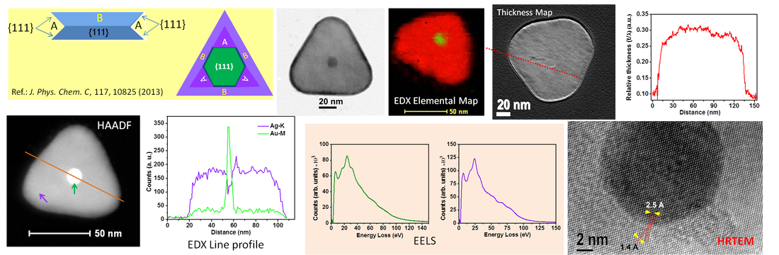
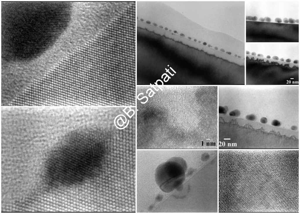
The appearance of different anisotropic one-dimensional (1D) and two-dimensional (2D) gold (Au) core−silver (Ag) shell nanostructures in a single reaction environment. High-resolution transmission electron microscopy (HRTEM) images taken from the core region of a core− shell nanostructure revealed the prominent presence of the hexagonal-shaped gold seed leading to formation of a triangular final particle. The HRTEM studies provide the direct experimental evidence of the “silver halide” model proposed by Sigmund et al. (Lofton, C.; Sigmund, W. Adv. Funct. Mater. 2005, 15, 1197−1208) to explain the kinetic growth mechanism behind their formation. It is important that this information cannot be identified from a single composite nanoparticle due to the lack of atomic number (Z) contrast difference. We have studied energy-dispersive X-ray line profile spectra and elemental mapping using the high-angle annular dark-field scanning/transmission electron microscopy (STEMHAADF) technique corresponding to the Au-M and Ag-K energies from the similar core−shell structures. This confirms the composition of the core to be made of gold and that of the shell of silver. The line profile along the relative thickness map of a hexagonal and triangular nanoplate obtained using energy-filtered TEM indicates the formation of nearly uniform 2D structures. The nearly equal thicknesses of the core and outside shell of a core−shell nanoplate measured using electron energy loss spectroscopy in STEM mode also confirm the 2D growth of a gold seed forming a triangular core−shell nanoplate. See J. Phys. Chem. C 2013, 117, 10825−10833 for details.
For Details:
Title: Direct Experimental Evidence of Nucleation and Kinetics Driven Two Dimensional Growth of Core-Shell Structures
Source: Journal of Physical Chemistry C 2013, 117, 10825−10833
Author(s): Tanmay Ghosh and Biswarup Satpati*
Title: Direct Experimental Evidence of Nucleation and Kinetics Driven Two Dimensional Growth of Core-Shell Structures
Source: Journal of Physical Chemistry C 2013, 117, 10825−10833
Author(s): Tanmay Ghosh and Biswarup Satpati*
Formation Mechanism of Hexagonal Monometallic Nanopaticles to Triangular Bimetallic Core-Shell Nanorings
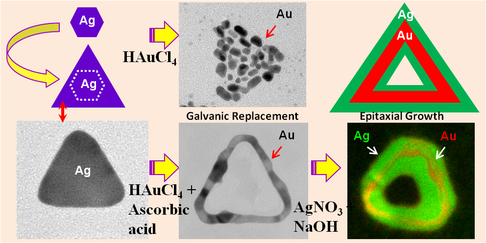
Using two-dimensional (2D) triangular silver nanoparticles as templates we first synthesized 2D triangular gold (Au) nanorings via galvanic replacement reaction and then overgrown Ag on Au nanorings via epitaxial growth process. Transmission Electron Microscopy (TEM) and associated techniques were used for in-depth characterization. TEM study reveals that single crystalline Ag nanoparticles led to the formation of continuous Au nanorings with single crystalline walls and the voids spaces which corroborate with the template shapes only when ascorbic acid was added to growth solution. Both the silver nanoplates and gold nanorings are having (111) planes as the basal planes. Subsequently we have synthesized Au-core — Ag-shell nanorings using previously synthesized Au nanorings as template. Energy dispersive X-ray (EDX) line profile spectra and imaging along with high-angle annular dark field scanning/ transmission electron microscopy (STEM-HAADF) techniques were used extensively for compositional study in addition to energy filtered TEM (EFTEM) imaging.
For Details:
Title: Characterization of Bimetallic Core-Shell Nanorings Synthesized via Ascorbic Acid Controlled Galvanic Displacement followed by Epitaxial Growth
Source: Journal of Materials Chemistry C, 2014, 2, 2439
Author(s): Tanmay Ghosh, Biswarup Satpati*, Dulal Senapati
Title: Characterization of Bimetallic Core-Shell Nanorings Synthesized via Ascorbic Acid Controlled Galvanic Displacement followed by Epitaxial Growth
Source: Journal of Materials Chemistry C, 2014, 2, 2439
Author(s): Tanmay Ghosh, Biswarup Satpati*, Dulal Senapati
Tilt Boundaries Induced Heteroepitaxy for Chemically Grown Dendritic Silver Nanostructures on Germanium and Their Optical Properties
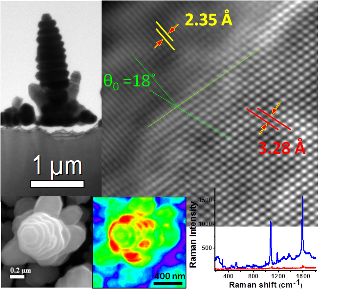
Dendritic silver nanostructures were prepared by a simple dip-and-rinse galvanic displacement reaction directly on germanium surfaces. The formation and evolution of these dendrites were investigated using scanning electron microscopy (SEM), high-resolution transmission electron microscopy (HRTEM) and energy-dispersive X-ray spectroscopy (EDX). The present results clearly show a new kind of heteroepitaxy, where large lattice mismatch between silver and germanium is accommodated at the interface by the formation of low-energy asymmetric tilt boundaries. Over grown sample relax strain by introducing crystal defects. Additionally, employing cathodoluminescence (CL) spectroscopy and imaging in a field emission gun scanning electron microscope (FEG-SEM), we provide information of surface plasmon assisted photon emission from a stack of Ag hexagon nanostructure. Surface enhanced Raman scattering (SERS) study shows the suitability of such Ag nanodendrite structures to be used as SERS active substrate.
For Details:
Title: Tilt Boundaries Induced Heteroepitaxy for Chemically Grown Dendritic Silver Nanostructures on Germanium and Their Optical Properties
Source: Physical Chemistry Chemical Physics, 2014, 16, 16730
Author(s): Tanmay Ghosh, Pabitra Das, Tapas Kumar Chini, Tapas Ghosh and Biswarup Satpati*
Title: Tilt Boundaries Induced Heteroepitaxy for Chemically Grown Dendritic Silver Nanostructures on Germanium and Their Optical Properties
Source: Physical Chemistry Chemical Physics, 2014, 16, 16730
Author(s): Tanmay Ghosh, Pabitra Das, Tapas Kumar Chini, Tapas Ghosh and Biswarup Satpati*
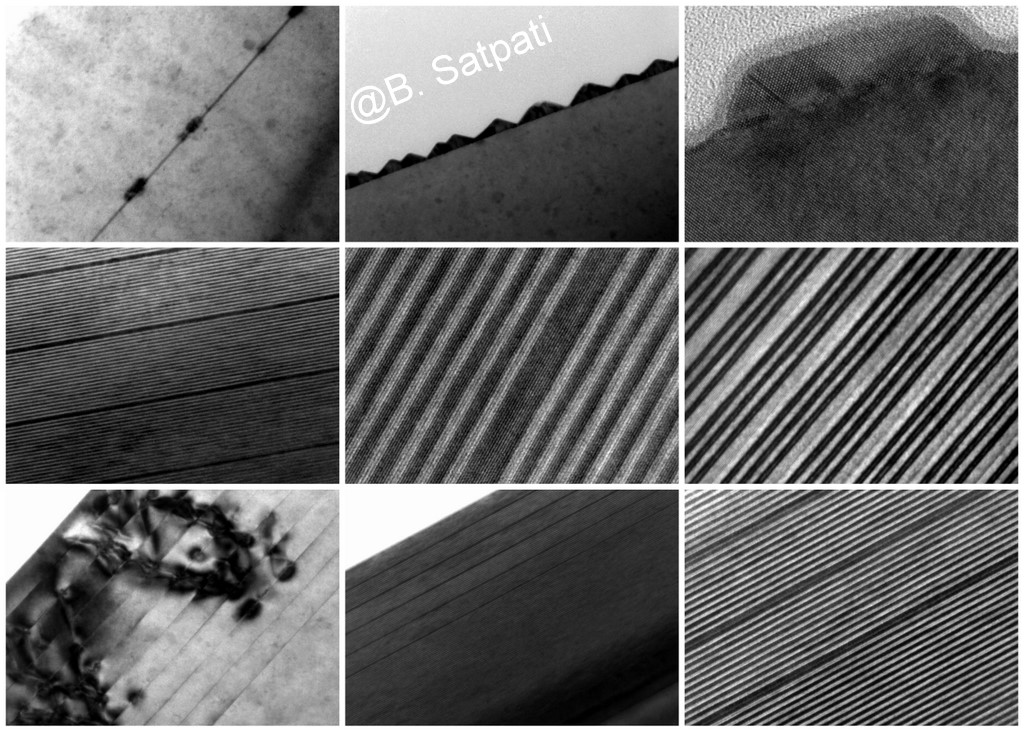
Study of inelastic mean free path of metal nanostructures using energy filtered transmission electron microscopy imaging
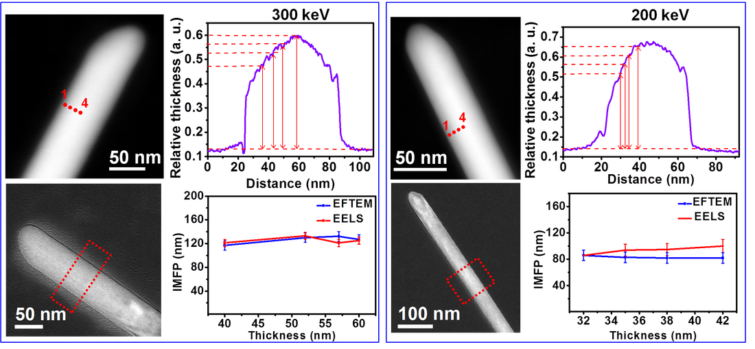
We report a simple method for measuring the inelastic mean free path of nanostructures of known geometry using energy filtered transmission electron microscopy imaging. The mean free path of inelastic electrons was measured by using systems having known symmetry, such as cylindrical or cubic, combined with Poisson statistics without employing the knowledge of microscope parameters, namely the convergence angle and the collection angle.Having inherent symmetry of such systems, their absolute thickness can be measured from their two-dimensional projection images. We have calculated mean free path of inelastic scattering of electrons in gold, silver and nickel doing case study research by employing gold nanorod, silver nanocube and nickel nanorod lying on a carbon-coated TEM grid at two different electron energies (viz. 200and300keV) following this alternative approach. Results obtained using such alternative approach were verified using microscope parameters.
For Details:
Title: Study of inelastic mean free path of metal nanostructures using energy filtered transmission electron microscopy imaging
Source: Journal of Microscopy, Vol. 258, Issue 3 2015, pp. 253–258
Author(s): T. GHOSH, M. BARDHAN, M. BHATTACHARYA & B. SATPATI*
Title: Study of inelastic mean free path of metal nanostructures using energy filtered transmission electron microscopy imaging
Source: Journal of Microscopy, Vol. 258, Issue 3 2015, pp. 253–258
Author(s): T. GHOSH, M. BARDHAN, M. BHATTACHARYA & B. SATPATI*
Using a FEI, TECNAI G2 F30, S-TWIN microscope
Attachments:
1. High-angle annular dark field (HAADF) detector from Fischione (model 3000)
2. Electron Energy Loss Spectroscopy (EELS) using Gatan Quantum SE (model 963)
3. Energy dispersive X-ray spectroscopy (EDS) using EDAX Instruments
Attachments:
1. High-angle annular dark field (HAADF) detector from Fischione (model 3000)
2. Electron Energy Loss Spectroscopy (EELS) using Gatan Quantum SE (model 963)
3. Energy dispersive X-ray spectroscopy (EDS) using EDAX Instruments
May, 2005- June, 2007: Post-doctoral Researcher at Paul Drude Institute for Solid State Electronics, Berlin, Germany with Dr. Achim Trampert
Project title: Antimonide Quantum-Dots for Mid-Infrared Nano-Photonic Devices (DOMINO): The 3–5 µm window of the mid-IR wavelength range is the window of choice for developing photonic-based products with important societal impact such as photonic sensors for environment monitoring, photonic diagnosis devices for health care, laser assisted surgery, free-space optical communication systems,… However, there is actually a lack of suitable laser diodes (LDs) operating in this domain. The main objective of this project was to demonstrate the feasibility of antimonides-based quantum-dots (QDs) nano-photonic lasers operating continuous wave (cw) at room temperature (RT) in the 3–5 µm wavelength range.
The project encompasses diverse technological as well as theoretical steps (such as, e.g., epitaxial growth, structural and electro-optical investigations, high-fidelity quantummechanical modeling, device design, processing and testing,). My job in this project was to characterize the microstructure (shape, size, density, lateral and vertical arrangement of QDs), the chemical composition, and the strain relaxation mechanisms of QD heterostructures and buried layers with nanometer resolution using high-resolution transmission electron microscopy (HRTEM) techniques.
The project encompasses diverse technological as well as theoretical steps (such as, e.g., epitaxial growth, structural and electro-optical investigations, high-fidelity quantummechanical modeling, device design, processing and testing,). My job in this project was to characterize the microstructure (shape, size, density, lateral and vertical arrangement of QDs), the chemical composition, and the strain relaxation mechanisms of QD heterostructures and buried layers with nanometer resolution using high-resolution transmission electron microscopy (HRTEM) techniques.
Publications from this research:
[10] Title: Interfacial intermixing in InAs/GaSb short-period-superlattices grown by molecular beam epitaxy
Author(s): Luna, E; Satpati, B; Rodriguez, JB, et al.
Source: APPLIED PHYSICS LETTERS Volume: 96 Issue: 2 Article Number: 021904 Published: 2010
[9] Title: Interface properties of (Ga,In)(N,As) and (Ga,In)(As,Sb) materials systems grown by molecular beam epitaxy
Author(s): Luna, E; Ishikawa, F; Satpati, B, et al.
Source: JOURNAL OF CRYSTAL GROWTH Volume: 311 Issue: 7 Pages: 1739-1744 Published: 2009
[8] Title: Transmission Electron Microscopy Study of Sb-Based Quantum Dots
Author(s): Satpati, B; Tasco, V; Deguffroy, N, et al.
Conference Information: 15th Conference on Microscopy of Semiconducting Materials, Date: APR 02-05, 2007 Univ Cambridge Cambridge ENGLAND
Source: MICROSCOPY OF SEMICONDUCTING MATERIALS 2007 Volume: 120 Pages: 251-254 Published: 2008
[7] Title: Type II transition in InSb-based nanostructures for midinfrared applications
Author(s): Intartaglia, R; Raino, G; Tasco, V; Satpati, B, et al.
Source: JOURNAL OF APPLIED PHYSICS Volume: 103 Issue: 11 Article Number: 114516 Published: 2008
[6] Title: Investigations of InSb-based quantum dots grown by molecular-beam epitaxy
Author(s): Deguffroy, N; Tasco, V; Baranov, AN; Satpati, B, et al.
Source: Physica Status Solidi C - Current Topics in Solid State Physics, Vol 4, No 5 Volume: 4 Issue: 5 Pages: 1743-1746 Published: 2007
[5] Title: Molecular-beam epitaxy of InSb/GaSb quantum dots
Author(s): Deguffroy, N; Tasco, V; Baranov, AN; Satpati, B, et al.
Source: JOURNAL OF APPLIED PHYSICS Volume: 101 Issue: 12 Article Number: 124309 Published: 2007
[4] Title: Interface analysis of InAs/GaSb superlattice grown by MBE
Author(s): Satpati, B; Rodriguez, JB; Trampert, A, et al.
Source: JOURNAL OF CRYSTAL GROWTH Volume: 301 Pages: 889-892 Published: 2007
[3] Title: High-density InSb-based quantum dots emitting in the mid-infrared
Author(s): Tasco, V; Deguffroy, N; Baranov, AN; Satpati, B, et al.
Source: JOURNAL OF CRYSTAL GROWTH Volume: 301 Pages: 713-717 Published: 2007
[2] Title: Structural and optical properties of InSb quantum dots for mid-IR applications
Author(s): Tasco, V; Deguffroy, N; Baranov, AN; Satpati, B, et al.
Source: PHYSICA STATUS SOLIDI B-BASIC SOLID STATE PHYSICS Volume: 243 Issue: 15 Pages: 3959-3962 Published: 2006
[1] Title: High-density, uniform InSb/GaSb quantum dots emitting in the midinfrared region
Author(s): Tasco, V; Deguffroy, N; Baranov, AN; Satpati, B, et al.
Source: APPLIED PHYSICS LETTERS Volume: 89 Issue: 26 Article Number: 263118 Published: 2006
Using a JEOL JEM-3010 microscope
Attachments: GATAN slow-scan charge-coupled device camera.
Attachments: GATAN slow-scan charge-coupled device camera.
July, 2000- May, 2005: Ph. D at Institute of Physics, Bhubaneswar, with Prof. B. N. Dev
Thesis title: Ion irradiation effects in nanostructures grown on semiconductor surfaces
Metal nanostructures (e.g. Au, Ag, and Pt) and semiconductor nanostructures (e.g. Ge) on Si surfaces have been grown by resistive heating, e-beam evaporation as well as molecular beam epitaxy (MBE) under ultrahigh vacuum (UHV) conditions.
These nanostructures have been irradiated by Au ions with different energies (a few tens of keV - a few MeV). We have observed novel phenomena of sputtering, cratering, subsurface mixing (silicide formation) in nanometer scale and burrowing effect of nanoislands under different experimental conditions.
The sputtered particles were collected on catcher foils. Irradiated samples and the catcher foils have been analyzed by high-resolution transmission electron microscopy (HRTEM) in planer and cross-sectional geometries, Atomic force microscopy (AFM) and Rutherford backscattering spectrometry (RBS).
We have proposed and demonstrated a new method of replicating nanostructures on Si surfaces using metal nanoparticles on Si as mask and low energy ion-irradiation.
Publications from this research:
[7] Title: Energy dependent sputtering of nanoclusters from a nanodisperse target
Author(s): Satpati, B; Ghatak, J; Joseph, B, et al.
Source: NUCLEAR INSTRUMENTS & METHODS IN PHYSICS RESEARCH SECTION B Volume: 244 Issue: 1 Pages: 278-282 Published: 2006
[6] Title: Size distribution of sputtered particles from Au nanoislands due to MeV self-ion bombardment
Author(s): Satpati, B; Ghatak, J; Satyam, PV, et al.
Source: JOURNAL OF APPLIED PHYSICS Volume: 98 Issue: 6 Article Number: 064904 Published: 2005
[5] Title: Replicating nanostructures on silicon by low-energy ion beams
Author(s): Satpati, B; Dev, BN
Source: NANOTECHNOLOGY Volume: 16 Issue: 4 Pages: 572-578 Published: 2005
[4] Title: Ion-beam-induced embedded nanostructures and nanoscale mixing
Author(s): Satpati, B; Satyam, PV; Som, T, et al.
Source: JOURNAL OF APPLIED PHYSICS Volume: 96 Issue: 9 Pages: 5212-5216 Published: 2004
[3] Title: Nanoscale ion-beam mixing in Au-Si and Ag-Si eutectic systems
Author(s): Satpati, B; Satyam, PV; Som, T, et al.
Source: APPLIED PHYSICS A-MATERIALS SCIENCE & PROCESSING Volume: 79 Issue: 3 Pages: 447-451 Published: 2004
[2] Title: Energy spike induced effects in MeV ion-irradiated nanoislands
Author(s): Satpati, B; Goswami, DK; Vaishnav, UD, et al.
Source: NUCLEAR INSTRUMENTS & METHODS IN PHYSICS RESEARCH SECTION B Volume: 212 Pages: 157-163 Published: 2003
[1] Title: Study of sputtered particles from gold nano-islands due to MeV self-ion irradiation
Author(s): Satpati, B; Goswami, DK; Roy, S, et al.
Source: NUCLEAR INSTRUMENTS & METHODS IN PHYSICS RESEARCH SECTION B Volume: 212 Pages: 332-338 Published: 2003
Using a JEOL JEM-2010 microscope
Attachments: GATAN slow-scan charge-coupled device camera.
Attachments: GATAN slow-scan charge-coupled device camera.
There are plenty of fun at the bottom!
"Never play with the feelings of others because you may win the game but the risk is that you will surely lose the person for a life time." --Shakespeare
